
X-ray analysis
An important tool for non-destructive analysis of electronic components (Transistors, capacitors, integrated circuits amd printed circuit boards) is the X-ray analysis. Here, the electronic components are x-rayed and the different degrees of absorption of X-ray quanta are measured with a detector. Therefore, it is possible, e.g. in integrated circuits, to visualize the course of bond wires and die-attach of crystals without damaging them or the potential error source. In circuit boards it is possible to check the quality of solder joints (Voids), vias etc.. The material of passive components like resistors and capacitors can be checked for cracks.
For non-destructive X-ray analysis we use the X-aminer from GE Sensing and Detection (previous Phoenix X-Ray). The voltage can be changed continously in the range from 20 kV to 160 kV. The different voltages directly influence the "hardness" of the beam. With this the absorption of the X-rays can be adjusted to the requirements of the examined components.
 IC in X-ray view.
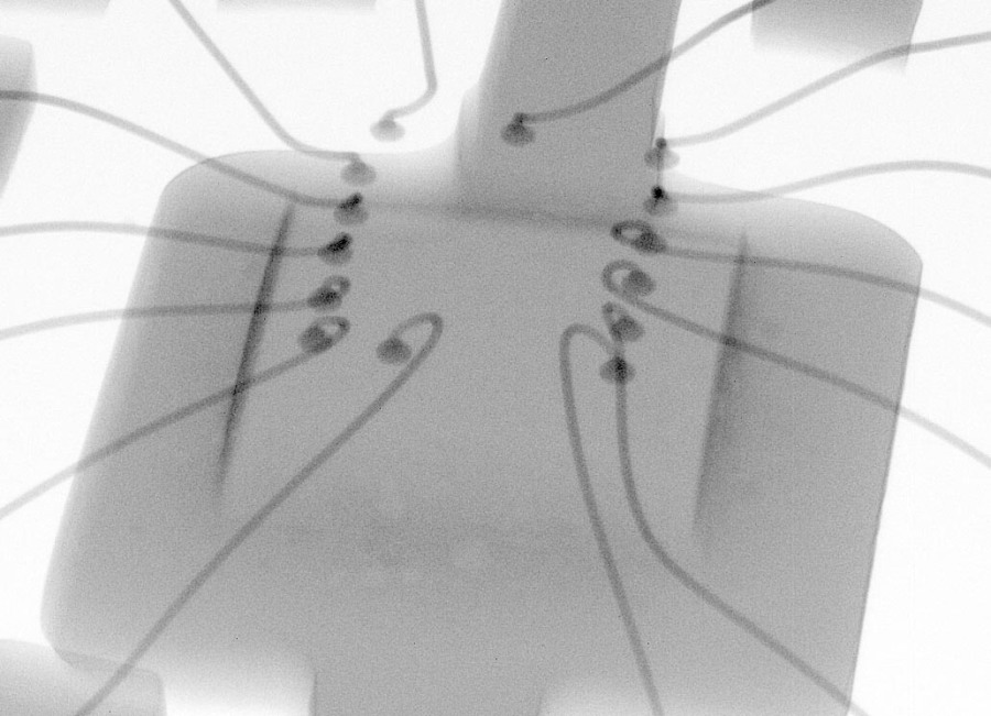 IC, short circuited of bond wires.
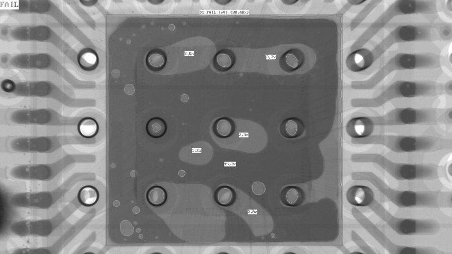
Additionally, this system offers an integrated option to calculate the area of voids in a solder joint. With this, one can make statements about the solder joint, the error in the joint and the security of it.
 IC in X-ray.
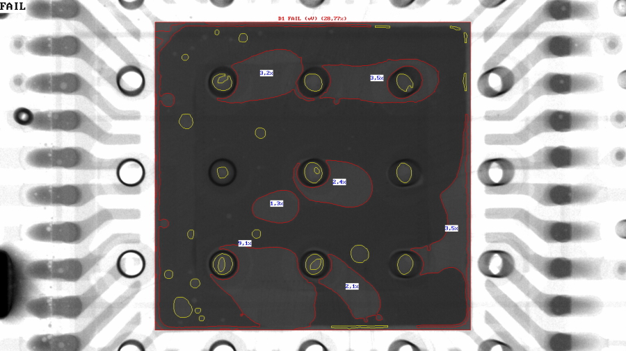
IC with void calculation (Void areas are marked with red and vias in yellow); The area covered by voids is larger than the specifications state.
© F/A Fehleranalyse Elektronik GmbH
Impressum Datenschutz Website Datenschutz Allgemein legal notice privacy policy