Material Analysis (EDAX)
The analysis of materials is done in the scanning electron microscope (SEM) with an energy dispersive x-ray system (EDX) of the company EDAX. The electron beam of the SEM is used to excite x-rays. The characteristic radiation of the x-rays is plotted according to their energy in a spectrum. Every element has a characteristic energy, and the elements can be assigned precisely to the material in question. Elements with a larger atomic weight than carbon can be distinguished with this method. The small size of the electron beam allows the analysis of rather small structures.
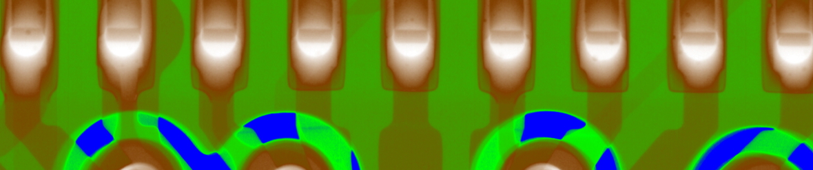
The image shows the surface of a printed circuit board. The board is faulty, as conductive bridges evolved between solder joints. The different elements of these conductive bridges were distinguished by EDAX.
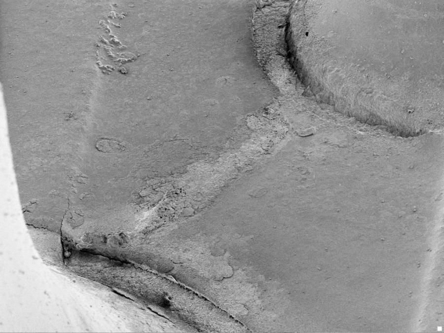
Solder joint on printed circuit board
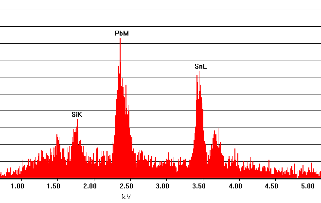
Detected elements on the bridge between the solder joints (dentrides)
© F/A Fehleranalyse Elektronik GmbH
Impressum Datenschutz Website Datenschutz Allgemein legal notice privacy policy